-

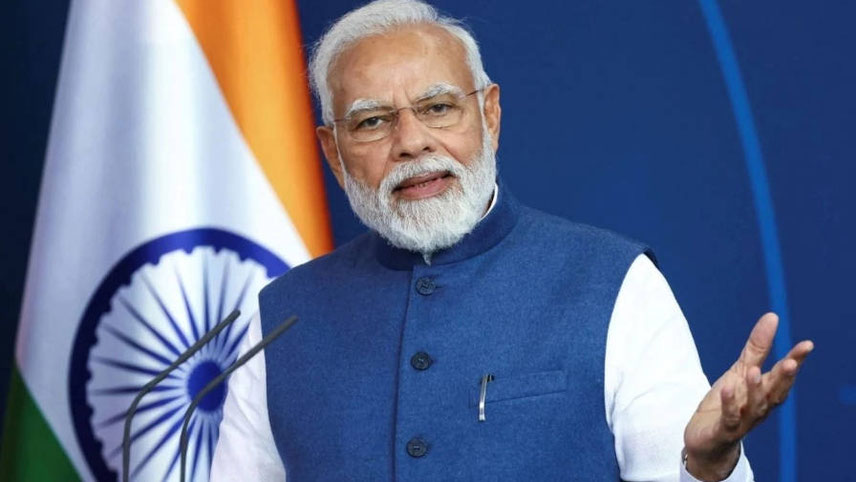
Modi: We are going to usher in a new era in electronics manufacturing
Last year, Japanese semi-conductor manufacturer Renesas Electronics Corporation, a premier supplier of advanced semiconductor solutions, entered into a strategic partnership with two Tata group companies -- TataMotors Ltd (TML) and Tejas Networks Ltd (Tejas). This strategic partnership is focussed on developing semiconductor solutions for technologies across automotive, IoT and 5G Systems.
n addition, Renesas and Tata Consultancy Services Limited (TCS) will also partner by establishing a Joint System Solution Development Centre in Bengaluru to focus on comprehensive system solutions for the IoT, Infrastructure, Industrial and Automotive segments by leveraging Renesas’ semiconductor solutions and TCS’ industry experience.
Tata appointee
Before onboarding Thakur, Tata Electronics had appointed Raja Manickam as CEO, Tata Electronics OSAT India, last year. OSAT/ ATMP is critical for India’s Semi-conductor Mission and overall semi-conductor ecosystem. No chip can be used in a product without going through the packaging and testing process. Also, for some very advanced products, packaging provides a way for integrating multiple chips done is different technologies into a simple package.
However, even after these developments, if the Tatas plan to apply for the semiconductor manufacturing scheme, the company will have to team up with a partner, ideally a fab manufacturer, who can transfer an existing, in-production technology, which has to be a production-grade license as per the government policy, as the group so far has no expertise in semi-conductor manufacturing.
However, the group’s other option is to develop the technology in-house, but this is a long, tedious and resource-hungry process. This is where a global chip manufacturer’s collaboration can make a difference. Will Thakur bring Intel as a possible technology partner? There is considerable speculation on this count.
Faltering effort
India’s attempts to emerge as a semi-conductor manufacturer have been faltering so far. The first round of applications for 28 nm fabs was open for a limited period of only 45 days, beginning January last year, which did not attract many applications. While the government hoped to receive applications from leading fabs such as Global Foundries, Intel, TSMC and Samsung, among others, all it received were semi-conductor fab applications from three consortiums, Vedanta-Foxconn, International Semiconductor Consortium (ISMC) and Singapore’s IGSS Ventures.
The three proposals did not make the cut, prompting the government to embark on further measures. It set up an advisory board with some top minds from the industry globally to guide the country in this important mission. And, in September 2022, the government modified the incentives in the semiconductor policy to make it more competitive by revising the incentives for all technology node slabs to a flat 50 per cent incentive.
The move to re-open the application window also stems from two unforeseen developments. ISMC had been counting Israeli chipmaker Tower as a tech partner in its $3 billion facility but this has been due to the company’s ongoing takeover by Intel. Tower has not been able to proceed to sign binding agreements as things remain under review after Intel acquired it for $5.4 billion last year.
The deal is pending regulatory approvals. The second mega $19.5 billion plan to build chips locally by a joint venture between India’s Vedanta and Taiwan’s Foxconn is also proceeding slowly as their talks to rope in European chipmaker ST Microelectronics as a partner are deadlocked.
-

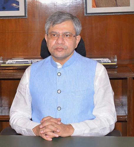
Vaishnaw: wooing chip-makers
ISM vetting plans
India Semi-conductor Mission (ISM), the nodal body now implementing the government’s semi-conductor manufacturing plan, went through the fine print of all three proposals. It has held back a formal announcement but official sources openly hint at their unviability, saying that since none of the proposals had come from existing semi-conductor manufacturers, making sustenance of these plants that much more critical in the long term. Caution appears to be the key to the government’s approach.
Ajai Chowdhry, co-founder, HCL, and adviser to the ISM, believes that the government should take a cautious approach in approving the country’s first semiconductor plant as its success is critical given the Centre and state governments will together contribute a 70 per cent subsidy for building it. “If India is going to give 70 per cent, the project should better work. If it fails, it reflects badly on the Indian government for taking the wrong decision. So, it’s become a bit scary in some manner to take this decision. So, the government is being extra careful in taking the steps ahead and rightfully so, because 70 per cent you’re giving, and if the project does not flower or work for India, it will be a big disaster,” he said in an open interview.
Apart from Chowdhry, ISM includes top minds in the semi-conductor space, including Vinod Dham and Ajit Minocha. So ISM has been looking at the business plans and feel these should deliver results with a proper cash flow planned out. They’re looking at the mix of technology, leadership and funding.
Newbies in forefront
“All proposals that have come are not from existing semiconductor manufacturers. That is the challenge…,” Chowdhry said. So, ISM is now advising the existing investee companies to finetune their proposals.
But, why have India’s dreams not panned out the way the government expected? For starters, none of the biggies in chipmaking – Intel, TSMC, Samsung, Global Foundries and Micron – applied for these incentives.
Secondly, even though a consortium of Vedanta and Taiwan’s Hon Hai Precision Industries (popularly known as Foxconn) was projected as the frontrunner, their credentials didn’t exactly inspire confidence. Hon Hai has expertise in making iPhones, not chips. And Vedanta’s a metals and mining player. It can set up manufacturing but not much else.
Also, advanced chips aren’t easy to make. Real expertise and specialisation is needed to set up these manufacturing facilities called ‘fabs’. There’s the complexity of printing really tiny circuits from the chip design to the silicon wafers. And as per a report by Credit Suisse, depending on what kind of chip it is, there could be anywhere between 400 to 1,400 steps in the manufacturing process.
Hiccups and challenges
So, any JV needs a tech partner with the know-how. And there have been serious hiccups on this front too. The end result is that the government isn’t quite happy with how things have turned out. Hence the move to reopen the scheme and try and lure in more applicants. After all, the government has $10 billion in incentives to dole out. But, it’s still not going to be easy. Because other countries want to become semi-conductor giants too and are lining up huge incentives and tax benefits. Just because everyone knows how crucial this segment is.
For instance, last year, the US passed the CHIPS (Creating Helpful Incentives to Produce Semi-conductors) Act with $50 billion in government subsidies. And they’re seeing results already. In December, TSMC committed to spending $40 billion to set up a fab in Arizona. And plans to launch one more in 2026 to create the most advanced chips ever.
-

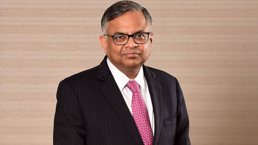
Chandrasekaran: Tatas have big plans for semiconductors
In 2021, South Korea, which is home to Samsung, announced a massive $450 billion plan to push chip manufacturing. And this year, even announced the ‘K Chips Act’ to nearly double the tax benefits for companies that wanted to make chips in the country. Even the EU has its own Chips Act with nearly $40 billion of subsidies.
Yes, things look tough. But we’re also not giving up that easily. Justifying the reopening of the applications and the changes being brought, Ajai Chowdhry says that the government had taken the right step in keeping the policy open and changing it to allow more mature nodes, beyond 40 nm, besides increasing the capital subsidy to 50 per cent from 30 per cent, making it the most attractive policy among countries like the US, Europe and China.
He feels that that India’s semiconductor plan should be de-politicised, where states and Centre should work together to set up specialised hubs, for instance, focusing on specific areas such as silicon semiconductor manufacturing in Dholera, Gujarat, and compound semiconductor manufacturing in Karnataka. Such a strategy will avoid duplication of infrastructure and investments from potential players, and will attract more investments.
Proposals needed
Besides, more proposals need to come in the compound semi-conductor space since India had huge requirements in sub-segments of power supplies for phones, computers, and electric vehicles. The investment in such plants would be in the range of $100-200 million versus billions of dollars needed for core semi-conductor manufacturing.
The challenge ahead, however, is fairly daunting. For one, the level of fiscal support envisioned is minuscule when one considers the scale of investments typically required to set up manufacturing capacities in the various sub sectors of the semiconductor industry. A semi-conductor fabrication facility, or fab, can cost multiples of a billion dollars to set up even on a relatively small scale and lagging by a generation or two behind the latest in technology.
Even granting that the PLI scheme intends to give only 50 per cent of the cost of setting up at least two greenfield semi-conductor fabs by way of fiscal support, not much of the current scheme outlay of about $10 billion is likely to be left to support other elements including display fabs, packaging and testing facilities, and chip design centres. Chip fabs also require millions of litres of clean water and stable power supply.
It may be best, if the new mission focusses fiscal support, for now, on other parts of the chip-making chain including design, where India already has considerable talent and experience. Indeed, even if we don’t become a manufacturing superpower, India could still make its mark somewhere in the value chain.


